and a pinout with inputs and outputs on opposite sides of the package. This arrangement greatly facilitates printed circuit board layout.
2010-07-13 16:39
performed from opposite ends of a fiber. Therefore, for calculating the true splice loss as anaverage figure and for accuracy reaso
2010-07-21 19:51
series devices and to offer a pinout with inputs and outputs on opposite sides of the package. This arrangement greatly facilitates printe
2010-07-17 22:55
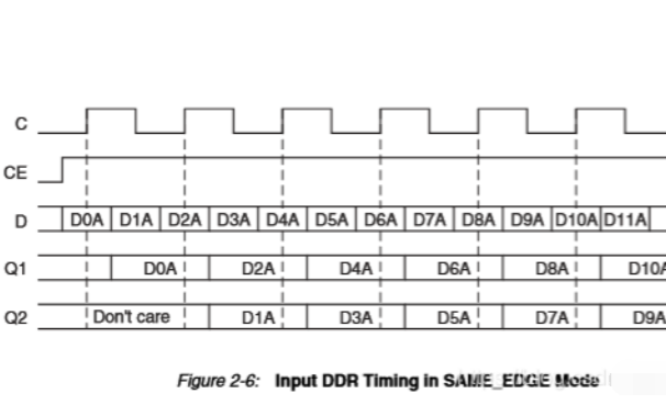
传统的输入DDR解决方案或OPPOSITE_EDGE模式是通过ILOGIC模块中的单个输入实现的。 数据在时钟的上升沿通过输出Q1提供给FPGA逻辑,在时钟的下降沿通过输出Q2提供给FPGA逻辑
2020-12-28 17:13
a pinout with inputs and outputs on opposite sides of the package. This arrangement greatly facilitates printed circuit board layout.
2010-07-13 16:28
with inputs and outputs on opposite sides of the package. This arrangement greatly facilitates printed circuit board layout. The 3
2010-07-17 22:45
Address;]If (Data field value == 1)[Selected register = 00000h;Data field value = 00000h;If (Opposite
2018-08-13 06:48
are orientedin the same direction in the ISO7220 and in opposite directions in the ISO7221. These devices have a logic inputand outp
2009-11-03 11:38
SN54ALS240A/ SN74ALS240A series and, at the same time, offer a pinout with inputs and outputs on opposite sides of the package. This arrangement gr
2010-07-11 15:44
These devices are ideal for driving bus lines or buffer memory address registers. They feature inputs and outputs on opposite si
2010-07-19 16:48