The effects of vias on PCB traces:Through the years we have worked with manyengineers who have had
2009-05-16 21:25
of vias on critical traces (such as fast rise time clock lines). These feelings haveranged from (a) the effects of vias are so negl
2009-03-24 14:10
the presence of vias on critical traces (such as fast rise time clock lines). These feelings have ranged from (a) the effects of vias
2010-01-15 10:12
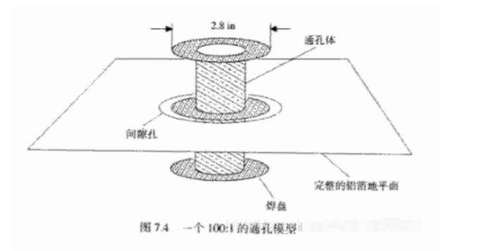
THE EFFECTS OF VIAS ON PCB TRACES
2009-03-27 15:45
在PCB设计中,盲孔和过孔是两种常见的孔类型,它们在电路板的制造过程中起着重要的作用。 定义 盲孔(Blind Vias
2024-09-02 14:47

PCB邮票孔的尺寸通常为0.020英寸或直径0.5毫米,会根据 PCB设计的而变化。PCB 邮票孔的尺寸由用于制造
2023-11-19 12:41

关于PCB 邮票孔、PCB 邮票孔设计要求 一、PCB 邮票孔是什么?
2023-11-07 10:52

一、PCB通孔:通常指印制电路板上的一个孔,用于固定安装插接件或连通层间走线。对于多层PCB来说,PCB通
2021-11-06 17:51
pcb通孔的孔径有哪些?pcb过孔和通孔区别 PCB通孔的孔径有很多种
2023-12-07 10:09
一、PCB通孔:通常指印制电路板上的一个孔,用于固定安装插接件或连通层间走线。对于多层PCB来说,PCB通
2022-07-30 17:32