functions such as buttons, scroll bars, and wheels. The sensors need only one PCB layer, enabling ultrathin applications.
2009-09-11 08:30
, scroll bars, and wheels. The sensors need only one PCB layer, enabling ultrathin applications.
2017-09-29 14:53
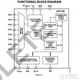
functions such as buttons, scroll bars, and wheels. The sensors need only one PCB layer, enabling ultrathin applications.The AD7147
2009-09-09 10:17
, scroll bars, and wheels.The sensors need only one PCB layer, enabling ultrathin applications. The AD7148 is an integrated capacita
2009-09-11 08:27
layer是什么?在PCB设计中layer是什么意思?PCB设计中多层板的层设置当初困扰了很久,就是没搞懂plane和layer
2019-10-16 11:37
to the die attach pad on the top PCB layer“,但是其他GND脚没有说明,参考设计里是全部与低部PAD相连了,我们按照参考设计即可吗
2020-04-29 07:42
AD中如何根据keep-out-layer层定义PCB板的形狀pdf下载
2018-01-25 17:18
plane是所有Layer的其中一个,Layer是指层,例如有常见的信号层Signal Layers——顶层印刷层和底层印刷层(也就是布线层),还有顶层丝印层、底层丝印层和禁止布线层等等,而
2017-11-09 14:59
plane是所有Layer的其中一个,Layer是指层,例如有常见的信号层Signal] Layer为正面,在这一层,画一根线就是画一条导线,即凡是走线的地方就表示有铜皮连接。
2019-05-26 09:00
Altium Designer中PCB各层的作用(1)Signal Layers(信号层)主要用于放置元件和走线。TopLayer:顶层,一般作为元件层。设计单面板时,元件层是不能布线的。双面板中元
2017-03-24 10:41