这是练习用的原理图,我已经在图中把VCC和GND走线宽度分别设置为30mil但是Design/update pcb后,自动布线,VCC和GND的走线却无变化,没有加粗,如下图,不知是怎回事
2016-01-05 00:35
怎么不能将原理图引入到PCB中那个Design|Update PCB是灰色的。
2014-06-06 08:23
Editor”窗口中设置规则,称为PCB准备第三步6.将原理图的网表导入到PCB中:在原理图文件中,点击下拉菜单[Design]-[Update
2018-03-12 10:05
本帖最后由 Innocencer 于 2016-6-12 16:52 编辑 Altium Design 10,电路图update pcb document时,报错差分信号找不到。net
2016-06-08 11:23
2014 TI MCU Design Days讲座PPT:MCU Software Update
2017-09-20 14:29
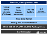
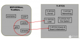
TI MCU Design Days讲座PPT:TI-RTOS Update: June
2017-10-24 14:42
the capture stage to the board layout stage is launched by selecting Design » Update PCB Document
2015-01-27 10:24
Altium Design 10,电路图update pcb document时,报错差分信号找不到。net not found in differential pair in current
2016-06-12 18:36
绘制①元器件放置、连线②统一修改或添加元器件封装,Tools → Footprint Manager③生成PCB,Design → Update PCB Documen
2019-07-09 07:32
PCB Design
2009-12-29 11:30